An article explains the function and principle of ky diode in detail-knowledge article
Date:2021-04-22Viewed:5101
Original title: ky diode function
ky diode is named by inventor Dr. ky, and SBD is short for SchotkyBarrierDiode (SBD). SBD is not made by using the principle of PN junction formed by contact between p-type semiconductor and n-type semiconductor, but by using the principle of metal-semiconductor junction formed by contact between metal and semiconductor. Therefore, SBD, also known as metal semiconductor (contact) diode or surface barrier diode, is a hot carrier diode.
ky diode action
ky diode is mainly used as a semiconductor device with low power consumption and ultra-high speed. The most remarkable feature is that the recovery time is extremely short (can be less than several nanoseconds), and the forward conduction voltage drop is only about 0.4V. It is mainly used for rectifying diodes, diodes and protection diodes with high frequency, low voltage and high current, and also used for rectifying diodes and small signal detection diodes in circuits such as microwave communication. Commonly used in communication power supply, frequency converter, etc.
The typical application is in the switching circuit of bipolar transistor to BJT. By connecting Shockley diode clamp to BJT, the transistor is close to the off state in the on state, which improves the switching speed of the transistor. This method is used for typical digital intelligent circuits such as 74LS, 74ALS and 74AS.
The biggest characteristic of ky diode is that the VF current is slightly smaller when the positive voltage drops. Under the same electrical condition, the drop of positive pressure is quite small. In addition, the recovery time is short. Low withstand voltage and large leakage current also have disadvantages. When choosing, we should consider it comprehensively.
ky diode principle
ky diode is a metal semiconductor device with rectifying characteristics by using noble metal (gold, silver, aluminum, platinum, etc.) A as positive electrode and N-type semiconductor B as negative electrode. Because there are a large number of electrons in N-type semiconductor and only a small number of free electrons in precious metal, electrons diffuse from high concentration B to low concentration A.. Obviously, metal A has no voids, and there is no diffusion movement of voids from A to B. With the diffusion of electrons from B to A, the concentration of electrons on the surface of B decreases gradually, and the electrical neutrality of the surface is destroyed, forming a momentum, and its electric field direction is B → A.. However, under the action of this electric field, the electrons in A also drift from A to B, which weakens the electric field formed by diffusion movement. When a space charge region with a certain width is established, the electron drift movement caused by electric field and the electron diffusion movement caused by different concentrations reach a relative balance, thus forming a ky barrier.
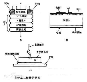
The typical internal circuit structure of ky rectifier is based on n- type semiconductor, on which an N-epitaxial layer with arsenic as a complexing agent is formed. The anode is made of molybdenum, aluminum and other materials. Silicon dioxide (SiO2 _ 2) is used to remove the electric field in the edge area and improve the pressure resistance of the pipeline. N-type substrate has smaller on-state resistance, and its mixed concentration is 100% higher than that of H layer. An N+ cathode layer is formed under the substrate, which can reduce the contact resistance of the cathode. By adjusting structural parameters, ky potential is formed between N-type substrate and anode metal, as shown in the following figure.
When forward bias voltage is applied to both ends of ky barrier (anode metal is connected to the positive pole of power supply and N-type substrate is connected to the negative pole of power supply), ky barrier layer narrows and its internal resistance decreases. On the contrary, if bias is applied to both ends of the ky barrier, the ky barrier layer becomes wider and its internal resistance becomes larger.
To sum up, the structure principle of ky rectifier is quite different from that of PN junction rectifier. Generally, the PN junction current tube is called junction current tube, while the metal semi-conductor tube is called ky rectifier tube. The Al-Si ky diode manufactured by silicon planar technology was also born. This can not only save precious metals, greatly reduce costs, but also improve the consistency of parameters.
The above content mainly introduces the function and principle ofky diode. If you need ky diode, please leave a message or call 0755-28100016; Massive ky diode inventory.
Shenzhen Shunhai Technology Co., Ltd. is a professional protection device such as fuses, chip fuses, ELLON resistors, chip resistors, chip inductors, integrated inductors, TVS, ESD, PPTC, GDT, TSS, MOS, LDO, etc. The electrostatic tube agent brands are Huade, Saruiwei, Shuokai, Tianer, Guoju, Housheng, Wangquan, TDK, and so on TAIYO, SUNLROP, TDK, LRC, ITE, SAMSUNG, professional sales teams and massive spot stocks provide customers with better service. Welcome to consult and cooperate.
Label: ky diode function, ky diode function and principle, ky diode function introduction, what is ky diode function